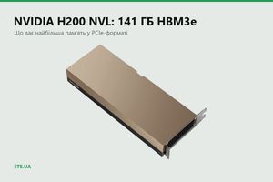
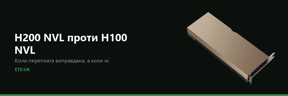
H200 NVL and H100 NVL are built on the same compute silicon: the same 835 TFLOPS in TF32, the same 3341 in FP8, the same 1785 MHz boost clock. Every difference between them sits in memory. So the question is not which card is faster, it is whether your workload is memory bound at all. If it is not, the premium buys nothing.
In brief
- Compute specs are identical at every precision, FP64 through INT8
- H200 NVL carries 1.5× the memory (141 GB against 94) and 1.22× the bandwidth (4813 against 3938 GB/s)
- Real workloads land anywhere from 0% to 3.4×: nothing on short BF16 prompts, 3.4× on a 32,000-token input
- MLPerf at a matched 700 W shows +28% on Llama 2 70B, not the headline 90%
- H200 NVL bridges up to four cards (564 GB), H100 NVL only two (188 GB)
Start with the fact that breaks most comparisons
Put the spec tables from NVIDIA's own product pages side by side and something turns up that reviews rarely mention. The compute side of the two cards matches to the last digit. Not roughly, exactly.
| Precision | H200 NVL | H100 NVL |
|---|---|---|
| FP64 | 30 TFLOPS | 30 TFLOPS |
| FP32 | 60 TFLOPS | 60 TFLOPS |
| TF32 Tensor Core | 835 TFLOPS | 835 TFLOPS |
| BF16 and FP16 Tensor Core | 1671 TFLOPS | 1671 TFLOPS |
| FP8 and INT8 Tensor Core | 3341 TFLOPS | 3341 TFLOPS |
| Boost clock | 1785 MHz | 1785 MHz |
Tensor Core figures include structured sparsity, as in NVIDIA's own footnote. Sources: H200 page, H100 page
The consequence is simple. When a job is limited by math, the two cards behave alike. That is not guesswork: in its MLPerf record write-up NVIDIA states that after TensorRT-LLM optimisations Llama 2 70B on H200 becomes compute bound, not bandwidth bound.
The whole difference lives in memory
| Spec | H200 NVL | H100 NVL |
|---|---|---|
| Capacity | 141 GB | 94 GB |
| Type | HBM3e | HBM3 |
| Bandwidth | 4813 GB/s | 3938 GB/s |
| Memory clock | 3201 MHz | 2619 MHz |
| Bus width | 6016-bit | 6016-bit |
| MIG profiles | up to 7 × 1g.18gb | up to 7 × 1g.12gb |
Sources: H200 NVL Product Brief, H100 NVL Product Brief, MIG profile reference. NVIDIA disagrees with itself on instance size: the product page says 16.5 GB, the documentation says 18
Both NVL cards run a wider bus than H100 SXM: six HBM stacks instead of five, which is why even the older H100 NVL reaches 3.9 TB/s against 3.35 on SXM. ServeTheHome worked through that part. Why capacity lands on 94 GB rather than a round 96, NVIDIA explains nowhere.
What that buys on actual workloads
There is no single number to quote. The spread runs from zero to 3.4×, according to how memory bound the job happens to be.
| Scenario | Gain | Measured by |
|---|---|---|
| Short context, 128 tokens, BF16 | around 0% | Baseten |
| Same test in FP8 | +11% | Baseten |
| Llama 2 70B, matched 700 W | +28% | MLPerf |
| Batch 4096, FP8 | +36% | Baseten |
| Batch 4096, BF16 | +47% | Baseten |
| HPC application suite, claim for NVL | up to 1.3× | NVIDIA |
| 32,784-token input, batch 64 | 3.4× | Baseten |
Baseten measured 8×H200 clusters against 8×H100 in SXM form, so carrying the ratio across to NVL comes with a caveat. Sources: Baseten, NVIDIA MLPerf blog, footnotes on the H200 page
Baseten's own conclusion is sharper than any slogan: outside those cases the H200 adds little over the H100, and plenty of inference workloads run cheaper on H100. For the NVL pair NVIDIA promises up to 1.7× on language models and up to 1.3× on HPC, while publishing no test conditions whatsoever.
How to read the numbers in the decks
The loudest figure in H200 material is “110X on HPC”. The footnote spells out the baseline: four GPUs against a pair of Sapphire Rapids 8480 processors. It is a CPU comparison. Against H100 on the same suite NVIDIA gives no combined figure at all: the footnote just lists the applications and compares one H100 SXM with one H200 SXM.
The second figure is 1.9× on Llama 2 70B. NVIDIA's footnote gives the conditions: H100 ran batch 8, H200 ran batch 32. Nothing is being rigged there, because the larger batch is exactly what the extra memory enables, and that is the point of the product. But 1.9× does not mean the same workload finishes in half the time. It means the card will hold a configuration its predecessor cannot. If your model already fits into 94 GB at the batch size you need, that gain never shows up on your invoice.
NVLink: the widest gap between the generations
| Spec | H200 NVL | H100 NVL |
|---|---|---|
| Cards per group | up to 4 | 2 only |
| Memory per group | 564 GB | 188 GB |
| NVLink bandwidth | 900 GB/s | 600 GB/s |
| Bridges per card | 1 wide, separate parts for 2 and 4 cards | 3 narrow, the same as on A100 PCIe |
Bridges from the two generations are not interchangeable. Sources: H200 NVL Product Brief, H100 NVL Product Brief, NVIDIA reference architecture
The rated 900 GB/s counts both directions. An owner running two H200 NVL cards in an HPE DL385 Gen11 posted the nvidia-smi output: 18 active links at 26.562 GB/s each, roughly 478 GB/s per GPU in one direction. The arithmetic holds. Cards outside a shared bridge group talk over PCIe Gen5 at 128 GB/s, about seven times slower.
What else changes besides speed
Swapping a card in a rack is not always painless. Here is the detail that cloud provider tables leave out.
| Spec | H200 NVL | H100 NVL |
|---|---|---|
| Default board power | 600 W | 400 W |
| Operating ambient temperature | 10-45 °C | 0-50 °C |
| Minimum driver | R565 TRD1, CUDA 12.7 | R535, CUDA 12.2 |
| UEFI | supported | not supported |
| NVIDIA AI Enterprise license | 5 years included | 5 years included |
Sources: Product Briefs for both cards, the H200 NVL announcement at SC24. Dell lists H200 NVL as a 450-600 W card, while the hardware floor in the Product Brief is 200 W
Look at the second row. The newer card draws 200 W more and tolerates a narrower ambient range at both ends. In a purpose-built machine hall that is trivia. In an office server room that climbs past 45 degrees in summer it is a reason not to buy. Electricity adds to it: 200 W of difference running around the clock comes to 1752 kWh per card per year.
When the premium pays back, and when H100 NVL is enough
The rule takes one step of arithmetic. The premium is justified when the gain on your workload profile, in percent, exceeds the price difference, in percent. Card costs 40% more, and you run a chat with short prompts at an 11% gain? Every token ends up more expensive than on H100 NVL. Push 30,000-token documents through in batches and a 3.4× gain covers the premium inside six months.
The second calculation matters more, and hardly anyone runs it. Compare configurations, not cards.
| Memory needed for weights and KV cache | What it means in practice |
|---|---|
| up to 94 GB | one H100 NVL. The premium buys memory you never touch |
| 94-141 GB | one H200 NVL, or a bridged pair of H100 NVL. One card means one slot instead of two and 600 W instead of 800 |
| 141-188 GB | a bridged pair of H100 NVL gives 188 GB |
| above 188 GB | H200 NVL only: a pair gives 282 GB, four give 564 GB. H100 NVL groups never go past two cards |
Derived from rated capacities and the maximum bridge group size in the Product Briefs for both cards
Now the case for buying when the cloud is right there. Rental wins on peak demand and one-off jobs, no argument. But both NVL cards ship with a five-year NVIDIA AI Enterprise license, which SXM buyers pay for separately. Data stays inside your perimeter, and for healthcare, finance and public sector projects that is a question of clearance rather than cost. One more thing: Hopper is winding down, and some server platforms carrying these GPUs have already closed their order books.
What we have in stock
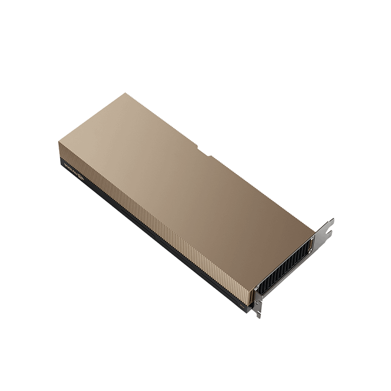
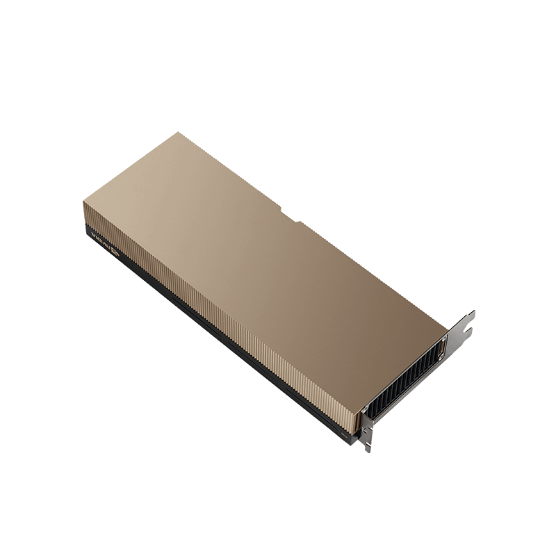
- PNY NVIDIA H200 NVL 141 GB HBM3e PCIe: retail packaging, in stock
- PNY NVIDIA H200 NVL 141 GB HBM3e PCIe, BLK version: identical hardware in bulk, for building servers in batches
- PNY NVIDIA H100 NVL 94 GB HBM3 PCIe: made to order, check lead times with the sales team
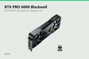
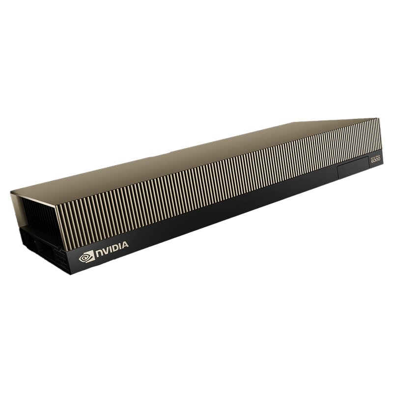
- PNY NVIDIA RTX PRO 6000 Blackwell Server Edition 96 GB: when HBM is overkill and 96 GB of GDDR7 covers the job
FAQ
Does the 94 GB H100 NVL work as a single card, with no bridge?
Yes. The question comes up constantly, because for a long time the card was shown exclusively in 188 GB pairs. ServeTheHome ran a separate piece on it, noting that publishing such a thing feels almost silly, yet so many sources online show the cards only in pairs that clarifying it was worth the trouble.
Will an H100 NVL bridge fit an H200 NVL?
No. H100 NVL uses three narrow bridges, the same ones as A100 PCIe. H200 NVL uses a single wide bridge of a new type, with separate part numbers for two-card and four-card groups. Refreshing a fleet means buying bridges again.
Does MIG work under KVM virtualisation without AI Enterprise? Can 56 profiles of 1g.18gb run on a server with eight GPUs?
That question went to the NVIDIA developer forum and never got an answer from the company. The 7×8 arithmetic works out, and the 1g.18gb profile is in the documentation. But “adds up on paper” and “validated by the vendor” are two different states.
Is vGPU through mdev supported on H200?
Going by owner reports on Proxmox VE 9, only SR-IOV is available: the mdev_bus and mdev_supported_types directories are absent, and nvidia-vgpu-mgr fails with a device binding error. An NVIDIA representative added on the forum that Proxmox-based KVM is not yet among the supported AI Enterprise platforms.
Is an InfiniBand switch required to connect two servers with H200 NVL?
An NVIDIA forum moderator answered this exact configuration (two GPUs in one server, four in the other) plainly: no switch is needed, wiring the ConnectX-7 adapters back to back is enough. The trap lies elsewhere. If the GPU and the network card land in different NUMA nodes, traffic routes through the CPU.
Does NVLink work inside a virtual machine?
One documented case exists: two H200 NVL cards in an HPE DL385 Gen11, Proxmox VE 8.4, VFIO passthrough, an Ubuntu guest, driver 580.95.05. All 18 links active inside the VM. The write-up adds candidly that Proxmox makes no official claim of NVLink support in VMs. The configuration runs, but it sits outside any guaranteed scenario.
These models are in our catalogue
Let us size this for your workload
Tell us the model, the context length and how many concurrent requests you expect. An engineer will calculate the memory you need, say whether one card covers it or a bridged group is required, and check compatibility with your platform.
Get a consultation